Introduction
Hello again, now on the new website! As a parting gift for some friends, I made an overly complicated CW beacon capable of reading morse code bits and flashing out through an LED. I will show the logic process, the schematic, and the PCB design.
Of course, this whole thing can be accomplished through a single Arduino. But this is way more fun.
Link to schematic and export files
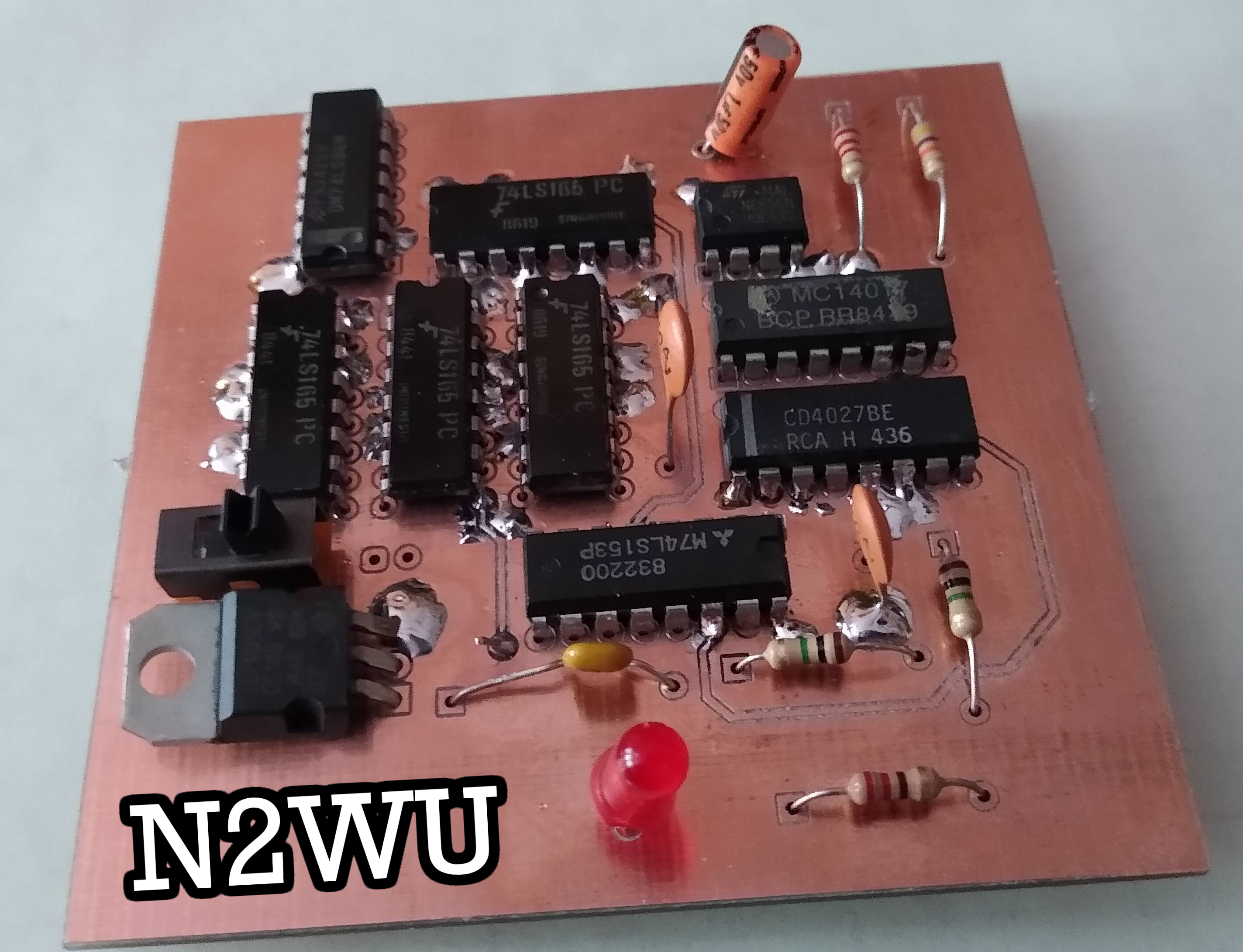 Finished Board
Problem Statement
What I needed was a board capable of CW output through an LED. I needed upwards of 33 bits to encode CW data (all series of clock pulses) out to an LED. I ended up going with 4 characters, which fits nicely with my simplified and “shortcutted” timing requirements.
How I decided to solve this was through shift registers, counters, timers, and flip flops. I used a decade counter (10) to iterate through the following steps:
| Clock Pulse | Event |
|---|---|
| 1 | Load Shift Registers |
| 2 | Bit 0 (LSB) |
| 3 | Bit 1 |
| 4 | Bit 2 |
| 5 | Bit 3 |
| 6 | Bit 4 |
| 7 | Bit 5 |
| 8 | Bit 6 |
| 9 | Bit 7 (MSB) |
| 10 | Flip-flop |
Integrated Circuits Used
555 Timer
A simple LM555CN Timer fed the clock pulses for this circuit, with a 47 k Ohm, 2.2k Ohm resistor, and a 0.1 and 1 uF capacitor.
74LS165
I used the 74LS165, or the 8-bit shift register, to load all my data. I used the following formula to hard-code all my CW output with bits:
CW Dit = 1 bit
CW Dah = 3 bits
CW Space = 1 bit
CW Character Space = 5 bits
CW Word Space = 7 bits
In my code, I cut off the character spaces since I only had 8 spaces. This is imperfect binary since characters like “O” are much longer than “i” or “e”. My bits for the word are simply wired +5V or GND, LSB from pin 1 on the 74LS165.
74LS153
This chip is the “train station” of the whole operation. As serial input flows from all 74LS165 chips, this is responsible for controlling what pin comes through and outputs directly to the LED. It relies on a JK flip-flop to select which character is selected.
74LS186
The 74LS186 is an exclusive-OR gate used to simply trigger the “LD” (active low) stage of the 74LS153, the multiplexer. I only use VCC and the 0th bit of the decade counter for the following truth table:
| 4017_Q1 | VCC | Output | Result |
|---|---|---|---|
| 0 | 1 | 1 | None |
| 1 | 1 | 0 | Active-Low LOAD |
CD4027
This is the JK flip flop required for selecting the chip. On the 10th clock pulse, this device increments from 0-3 to select one of the characters. Looks further into the schematic portion for how this works. I used this reference for storing bits.
CD4017
This is the decimal 10-bit decade counter. It very simply gives me an output on bits 0-9 on a rotation so I can load on trigger 0, execute on 1-6, then switch on bit 7.
Schematic
Below you’ll find the completed schematic on Multisim
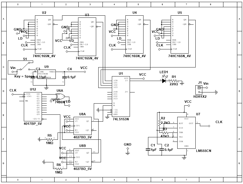 Full Schematic
Now, I’ll break it down with some explanation:
Data Storage
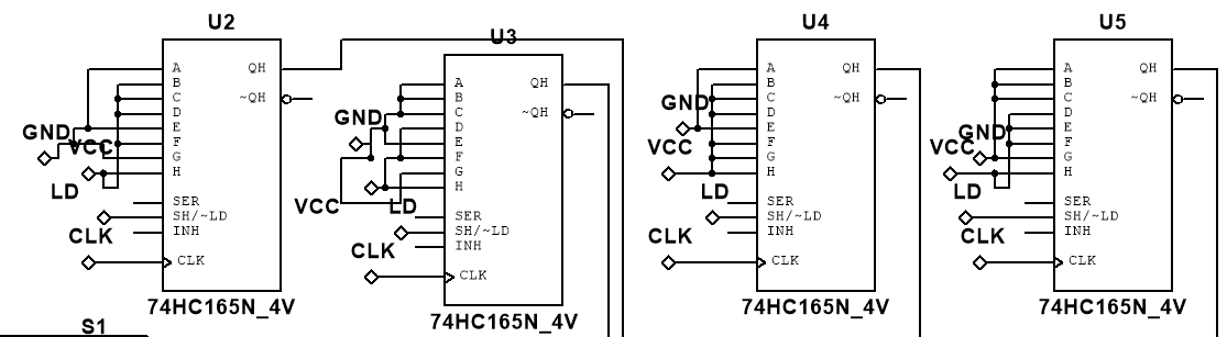 Data stored in 3 shift registers. It is either hardcoded with +5V (1) or GND (0). The CLK comes from the 555 timer.
Increments and Multiplexing
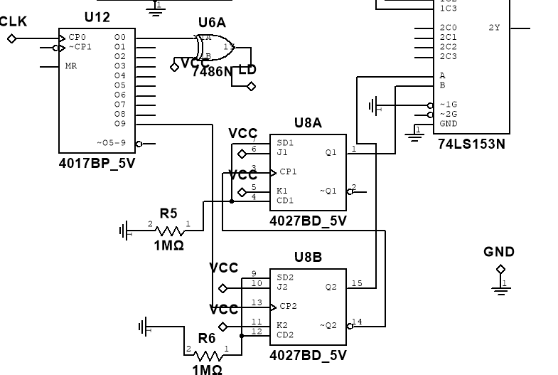 Here you can see the decade counter (4017) fed to the LD input of the 4 shift registers. using an XOR gate. Further, you can see the JK Flip-flops with the 4027 to increment the binary counter on the 153.
PCB Design
After schematic design and virtual validation, I went right to designing the PCB. I decided to use two ground planes to get my +5V and GND readily available. I imagine this creates sort of a “giant capacitor” but with 5V and a wide separation the difference is negligible. Unfortunately due to this, I was soldering on the top and bottom of the board. I could not use headers of any kind due to the soldering, so be careful when you design boards like this.
Also, I recommend you take the board to a friend or lab to print. Costs for 5 boards exceeded $75 using the cheapest sources I know!
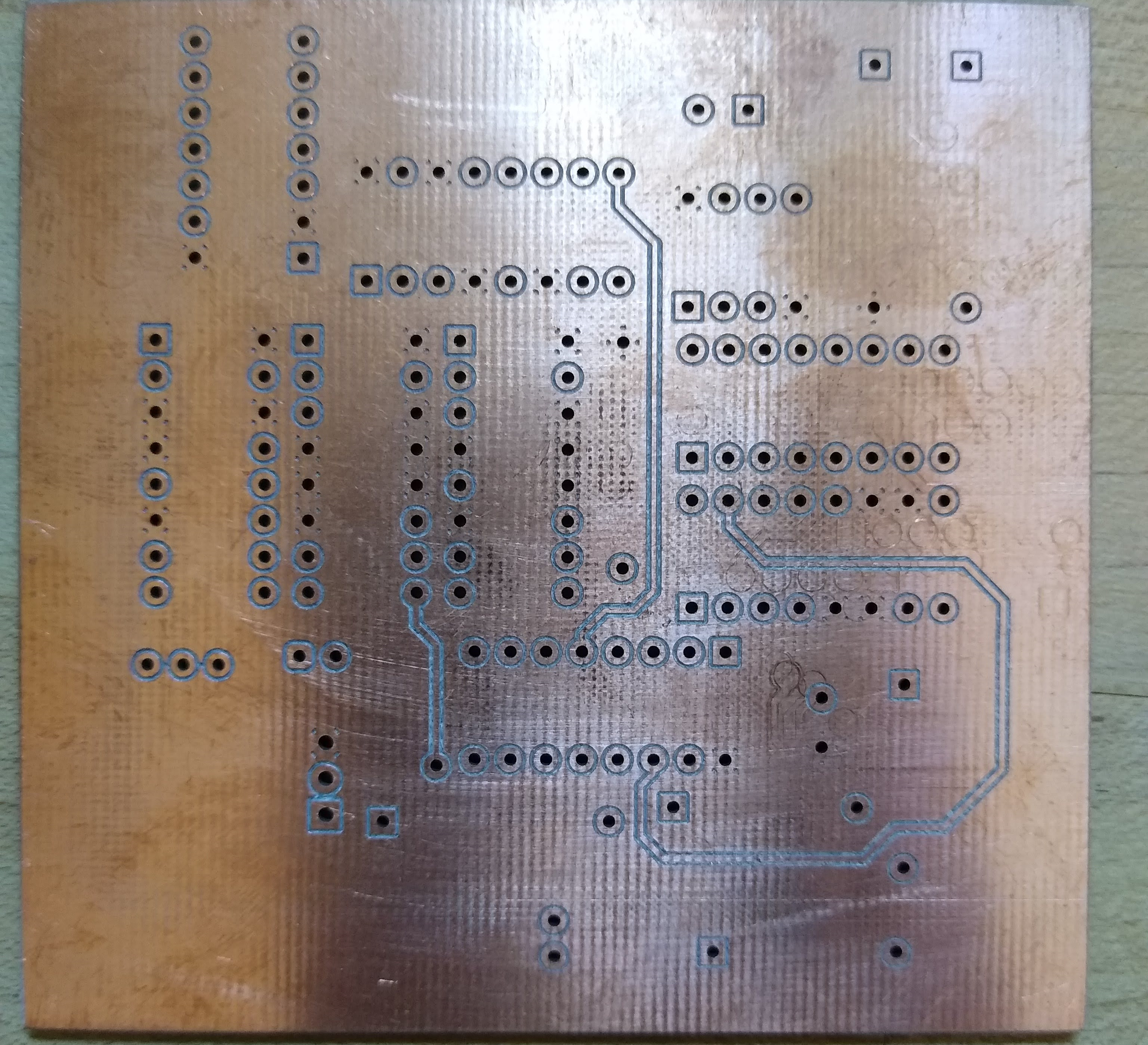 Top Layer of PCB. Note the ground plane and connections.
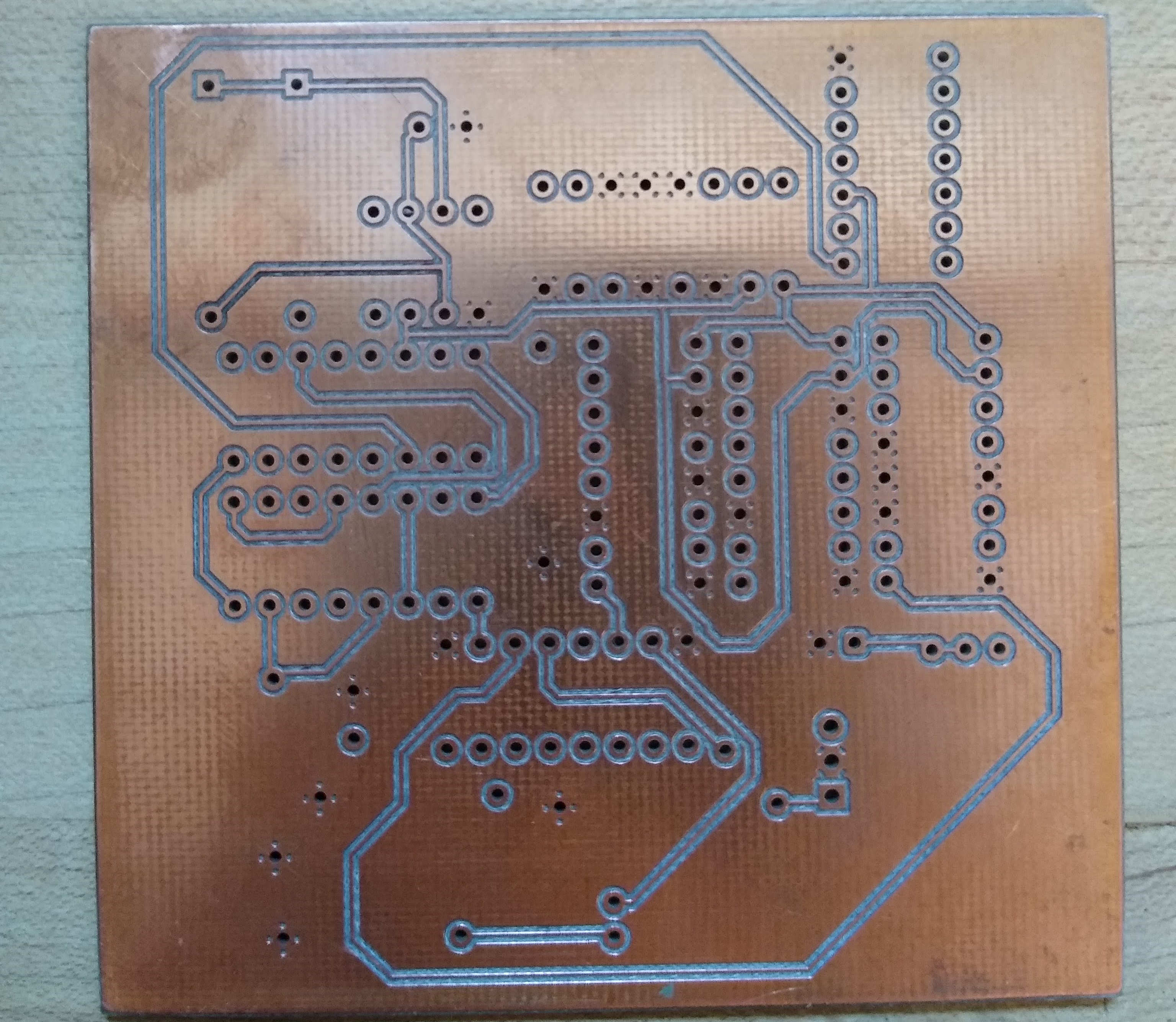 Bottom Layer of PCB. Note the ground plane and more connections.
Conclusion
Overall, the board can take in >6V and effectively function as a hardwired PCB beacon. I see this in the future adding stages to the front end; you could add a keyboard or selector buttons to control what happens with the bits. Also, use of a 16-parallel to serial converter would actually let you use all the morse characters available. Characters with two dahs and three total characters (like “G”) can’t fit on 8 bits.
Also, if I had more time I would 3D print a case, a stand, or something more presentable!

I hope you all enjoyed the move to the new website. I finally got it hosted using https://www.n2wu.com so this will be the permanent solution for as far as I can see. I already love the customization, security, speed, and user optimization!
-N2WU